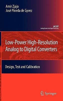
Low-Power High-Resolution Analog to Digital Converters: Design, Test and Calibration
暫譯: 低功耗高解析度類比轉數位轉換器:設計、測試與校準
Zjajo, Amir, Pineda de Gyvez, José
- 出版商: Springer
- 出版日期: 2010-11-05
- 售價: $2,470
- 貴賓價: 9.8 折 $2,420
- 語言: 英文
- 頁數: 293
- 裝訂: Hardcover - also called cloth, retail trade, or trade
- ISBN: 9048197244
- ISBN-13: 9789048197248
-
相關分類:
電路學 Electric-circuits
-
相關翻譯:
低功率、高分辨率的 A-D 轉換器 (簡中版)
海外代購書籍(需單獨結帳)
商品描述
With the fast advancement of CMOS fabrication technology, more and more signal-processing functions are implemented in the digital domain for a lower cost, lower power consumption, higher yield, and higher re-configurability. This has recently generated a great demand for low-power, low-voltage A/D converters that can be realized in a mainstream deep-submicron CMOS technology. However, the discrepancies between lithography wavelengths and circuit feature sizes are increasing. Lower power supply voltages significantly reduce noise margins and increase variations in process, device and design parameters. Consequently, it is steadily more difficult to control the fabrication process precisely enough to maintain uniformity. The inherent randomness of materials used in fabrication at nanoscopic scales means that performance will be increasingly variable, not only from die-to-die but also within each individual die. Parametric variability will be compounded by degradation in nanoscale integrated circuits resulting in instability of parameters over time, eventually leading to the development of faults. Process variation cannot be solved by improving manufacturing tolerances; variability must be reduced by new device technology or managed by design in order for scaling to continue. Similarly, within-die performance variation also imposes new challenges for test methods.
In an attempt to address these issues, Low-Power High-Resolution Analog-to-Digital Converters specifically focus on: i) improving the power efficiency for the high-speed, and low spurious spectral A/D conversion performance by exploring the potential of low-voltage analog design and calibration techniques, respectively, and ii) development of circuit techniques and algorithms to enhance testing and debugging potential to detect errors dynamically, to isolate and confine faults, and to recover errors continuously. The feasibility of the described methods has been verified by measurements from the silicon prototypes fabricated in standard 180nm, 90nm and 65nm CMOS technology.
商品描述(中文翻譯)
隨著CMOS製造技術的快速進步,越來越多的信號處理功能被實現在數位領域,以降低成本、降低功耗、提高良率和更高的可重構性。這最近對可以在主流深亞微米CMOS技術中實現的低功耗、低電壓的A/D轉換器產生了巨大的需求。然而,光刻波長與電路特徵尺寸之間的差異正在增加。較低的供電電壓顯著降低了噪聲裕度,並增加了製程、元件和設計參數的變異。因此,精確控制製造過程以維持均勻性變得越來越困難。在納米尺度上使用的材料固有的隨機性意味著性能將變得越來越不穩定,不僅在晶片之間,甚至在每個單獨的晶片內部。參數變異將因納米級集成電路的退化而加劇,導致參數隨時間的不穩定,最終導致故障的產生。製程變異無法僅通過改善製造公差來解決;必須通過新型元件技術來減少變異,或通過設計來管理,以便持續擴展。同樣,晶片內部性能變異也對測試方法提出了新的挑戰。
為了解決這些問題,《低功耗高解析度類比數位轉換器》專注於:i) 通過探索低電壓類比設計和校準技術的潛力,改善高速度和低雜散頻譜的A/D轉換性能的功率效率;ii) 開發電路技術和算法,以增強測試和除錯的潛力,動態檢測錯誤,隔離和限制故障,並持續恢復錯誤。所描述方法的可行性已通過在標準180nm、90nm和65nm CMOS技術中製造的矽原型的測量得到了驗證。
作者簡介
Amir Zjajo received the M.Sc. and DIC degrees from the Imperial College London, London, U.K., in 2000 and PhD degree from Eindhoven University of Technology in 2010, all in the electrical engineering. In 2000, he joined Philips Research Laboratories, Eindhoven, The Netherlands, as a member of the research staff in the Mixed-Signal Circuits and Systems Group. From 2006 until 2009, he was with Corporate Research of NXP Semiconductors as a senior research scientist. In 2009, he joined Delft University of Technology as a Faculty member in the Circuit and Systems Group. Dr. Zjajo has published more then 20 papers in referenced journals and conference proceedings, and holds 2 patents with 7 more pending. He serves as a member of Technical Program Committee of IEEE Design, Automation and Test in Europe Conference, and IEEE International Mixed-Signal Circuits, Sensors and Systems Workshop. His research interests include mixed-signal circuit design, signal integrity and timing and yield optimization of VLSI.
José Pineda de Gyvez received the Ph.d. degree from the Eindhoven University of Technology, The Netherlands, in 1991. From 1991 until 1999 he was a Faculty member in the Department of Electrical Engineering at Texas A&M University, USA. He is currently a Senior Principal at NXP Semiconductors in The Netherlands. Since 2006 he also holds the professorship "Deep Submicron Integration" in the Department of Electrical Engineering at the Eindhoven University of Technology. Dr. Pineda de Gyvez has been Associate Editor in IEEE Transactions on Circuits and Systems Part I and Part II, and also Associate Editor for Technology in IEEE Transactions on Semiconductor Manufacturing. He is also a member of the editorial board of the Journal of Low Power Electronics. Dr. Pineda has more than 100 combined publications in the fields of testing, nonlinear circuits, and low power design. He is (co)-author of three books, and has a number of granted patents. His work has been acknowledged in academic environments as well as in patent portfolios of many companies. Pineda's research has been funded by the Dutch Ministry of Science, US Office of Naval Research, US National Science Foundation, among others. Dr. Pineda is an IEEE Fellow.
作者簡介(中文翻譯)
Amir Zjajo 於2000年獲得英國倫敦帝國學院的碩士學位及DIC學位,並於2010年獲得埃因霍溫科技大學的博士學位,專攻電機工程。2000年,他加入荷蘭埃因霍溫的飛利浦研究實驗室,成為混合信號電路與系統組的研究成員。從2006年到2009年,他在NXP半導體的企業研究部擔任高級研究科學家。2009年,他加入代爾夫特科技大學,成為電路與系統組的教職員。Zjajo博士已在參考期刊和會議論文集中發表超過20篇論文,並擁有2項專利,另有7項專利正在審核中。他擔任IEEE歐洲設計、自動化與測試會議的技術程序委員會成員,以及IEEE國際混合信號電路、感測器與系統研討會的成員。他的研究興趣包括混合信號電路設計、信號完整性以及VLSI的時序和良率優化。
José Pineda de Gyvez 於1991年獲得荷蘭埃因霍溫科技大學的博士學位。從1991年到1999年,他在美國德州農工大學的電機工程系擔任教職。現在,他是荷蘭NXP半導體的高級首席。自2006年以來,他還在埃因霍溫科技大學的電機工程系擔任「深亞微米整合」的教授。Pineda de Gyvez博士曾擔任IEEE電路與系統期刊第一部分和第二部分的副編輯,並且是IEEE半導體製造期刊技術部分的副編輯。他也是《低功耗電子學期刊》的編輯委員會成員。Pineda博士在測試、非線性電路和低功耗設計領域擁有超過100篇的綜合出版物。他是三本書的(共同)作者,並擁有多項已授權專利。他的工作在學術界以及許多公司的專利組合中得到了認可。Pineda的研究得到了荷蘭科學部、美國海軍研究辦公室、美國國家科學基金會等機構的資助。Pineda博士是IEEE會士。


